Components
|
The best mail-order source of electronic components for a
hobbyist in the US is
Mouser Electronics.
They have no minimum on purchase and they charge for shipping
only once when there is a backorder. They were my primary
source. My secondary sources were
Newark Electronics, a local
electronics store and a local Radio Shack. Newark charges
separate shipping for every backorder and they are quite
indiscriminate in that. You end up receiving multiple (can be
10) shipments
of parts valued e.g. at 20c or 50c and $3.50 shipping charges
tacked
on top of those. If you order from Newark, make sure that you
disallow the backorders.
|
Circuit Board
|
I decided to move the power transistor, driven by the Maxim
chip, out of the board and to attach it to the circuit housing
letting the housing to serve as a heat sink. Moreover, I
decided to use Molex (alternative are AMP) wire to board
connectors for the connections to the transistor, adapter
socket, switch, the two LEDs, batteries, dynamo and light.
Finally, the
three chips and two relays were to be placed in sockets. The
purpose was to have sufficient flexibility in what was to be
an experimental design.
|

|
For a general discussion of the printed
circuit boards see the
site of Harry Lythall.
I decided to go with a double sided board. First, I designed
the layout on a 0.1" grid paper. While designing, I was
inserting the components into a 0.1" perforated board testing
how the layout was playing out. The size of the board I ended
up adopting was 2_5/8 x 2_1/8". Following Harry's suggestion,
I used the grid paper layout to mark holes on still another
perforated board. That board I clamped together with the
copper
clad board to drill holes.
Note: you should drill
the holes from bottom up as the copper sticks out from the
board in the direction of drilling, in the immediate vicinity
of a hole. Regrettably, I did not follow this rule as may be
apparent in the enclosed photographs. Upon drilling holes in
the clad board, I marked
connections with an etch resistant pen.
Etching was a relatively easy
process.
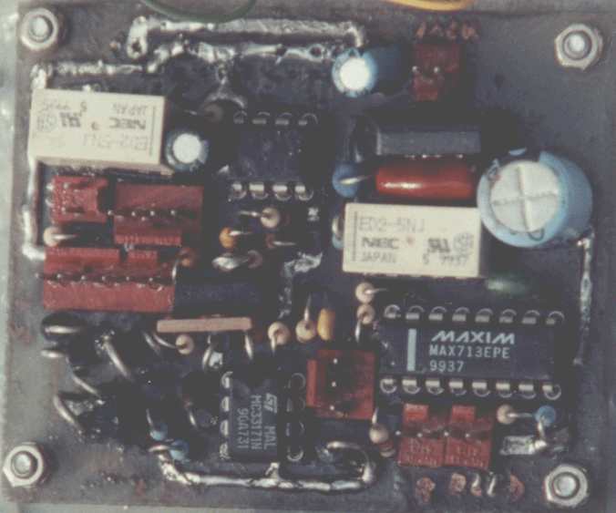
The designing of the layout turned out to take far more time than I expected, in fact a fortnight worth of evenings or so. The shown design was developed for the first version of the circuit. The charger circuit around MAX713 occupies the right side of the board. The protective part of the circuit, eventually removed, was placed in the upper left horizontal strip, as looked from above. The rest has been devoted to the core regulator circuit. If the charger circuit were to be dropped, the board could be significantly reduced in size. Have I thought more, I would have realized that the top of the board connections work when the component has its terminal exposed above the board. This is in particular not true for chip sockets. Thus I ended up with some wire connections. In addition, I needed to add an RC snubber, indicated in the schematic, connecting the terminals of the second op-amp, that ended up below the board. The finished board is shown in the adjacent photograph. For protection from the weather influence I covered the board, from both sides, with a silicon conformal coating. When spraying the coating, it is essential to protect the connectors. From above, you may just spray so that the coating spreads underneath the components. The Molex connectors I used stick out quite a bit from the board. That is convenient for plugging them in and unplugging but otherwise wastes space. My first connector choice was JST but they were unavailable within retail in the US. |

|
|
|